A final year project on “the Analysis of 4 bit ALU” submitted by Vasu Singh (from The NorthCap University, Gurugram, Haryana) to extrudesign.com.

1. Introduction
In this project, we will build the heart of a simple 4-bit CPU, the ALU (Arithmetic Logic Unit).
Believe it or not, computers existed before microcontrollers and CPUs were around. They used to be built using discrete parts including simple ICs and transistors.
CPUs are arguably the center of modern electronics, whether it be a mobile device or a control circuit for a factory. But how do CPUs work? What goes on inside?
A CPU consists of three main sections: memory for variables (registers), control circuitry (microcode), and the ALU. The ALU (Arithmetic Logic Unit) is the part of a CPU that does calculations and condition testing.
For example, if you wish to add two binary numbers, it is the ALU that is responsible for producing the result. If your program needs to execute some code if two values are equal it is the ALU that performs the comparison between the values and then sets flags if the condition is met or not.
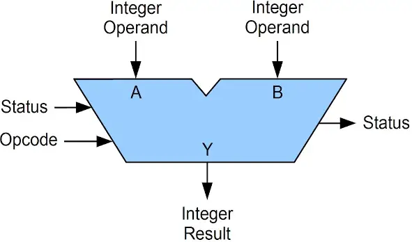
Modern CPUs consist of millions of transistors (even billions now!) and cannot possibly be duplicated at home. But a simple CPU (say, a Z80, for example) has only 8500 transistors. Computers in the past (such as many of the IBM mainframe computers) were built with discrete 4000 and 7400 series chips.
This means that we can build a CPU at home!!! So why wait?
This project will be a discrete 4-bit ALU that will be constructed with 7400 series chips.
2. Theoretical Analysis of 4 bit ALU
Because this project is rather complex you will need the following:
- Basic understanding of Combinational Circuits
- Basic understanding of Logic gates and their construction from universal gates
2.1 Combinational Circuits
2.1.1. Multiplexer (IC NO – 74151)
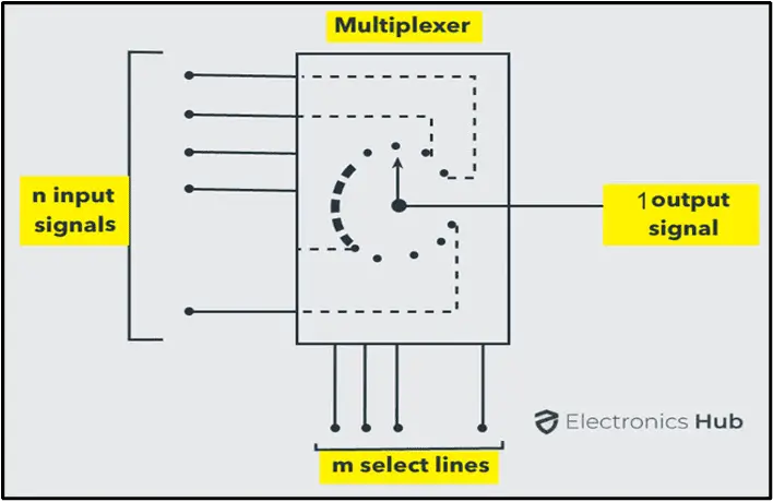
The multiplexer or MUX is a digital switch, also called a data selector. Circuit with more than one input line, one output line, and more than one selects line. It accepts the binary information from several input lines or sources and depending on the set of select lines, a particular input line is routed onto a single output line.
The basic idea of multiplexing is shown in the figure below in which data from several sources are routed to the single output line when the enable switch is ON. Therefore, multiplexers are also called ‘many to one’ combinational circuits.

The below figure shows the block diagram of a multiplexer consisting of n input lines, m selection lines, and one output line. If there are m selection lines, then the number of possible input lines is 2m.
2.1.2. Decoder Driver (IC NO – 7447)
The Decoder is an essential component in BCD to seven segment decoder A decoder is nothing, but a combinational logic circuit mainly used for converting a BCD to an equivalent decimal number.
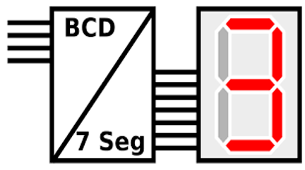
The circuit design, as well as operation, mainly depends on the concepts of Boolean algebra as well as logic gates.
A seven-segment LED display circuit can be built with eight LEDs. The common terminals are anode otherwise cathode. A general anode seven segment display includes 8 pins where 7-pins are input pins that are marked with from a to g & 8th-pin is connected to supply.
2.1.3. BCD Adder (Formed by 4-bit binary/parallel adders) (IC NO – 7483)
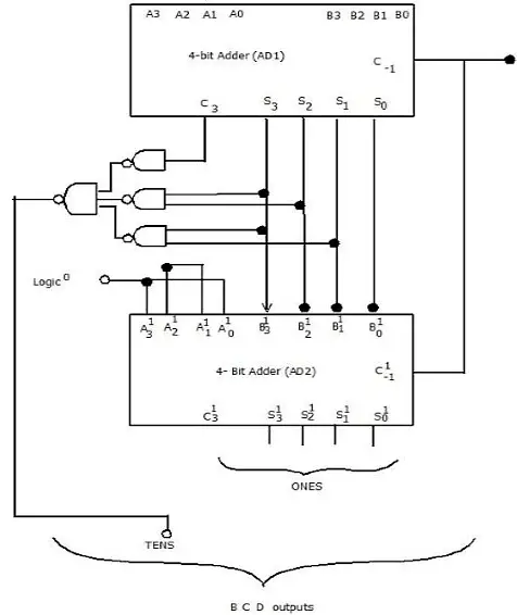
In this, if 4- bit sum output is not a valid BCD digit, or if carry C3 is generated, then decimal 6 (0 1 1 0) is to be added to the sum to get the correct result. The following fig shows 4-bit BCD Adder. BCD adder can be cascaded to add numbers several digits 1009 by connecting the carry out of a stage to the carry into the next stage.
2.2 Logic gates
A logic gate is a device that acts as a building block for digital circuits. They perform basic logical functions that are fundamental to digital circuits. Most electronic devices we use today will have some form of logic gates in them.
For example, logic gates can be used in technologies such as smartphones, tablets, or within memory devices.
In a circuit, logic gates will make decisions based on a combination of digital signals coming from its inputs. Most logic gates have two inputs and one output. At any given moment, every terminal is in one of the two binary conditions, false or true. False represents 0, and truly represents 1. Depending on the type of logic gate being used and the combination of inputs, the binary output will differ.
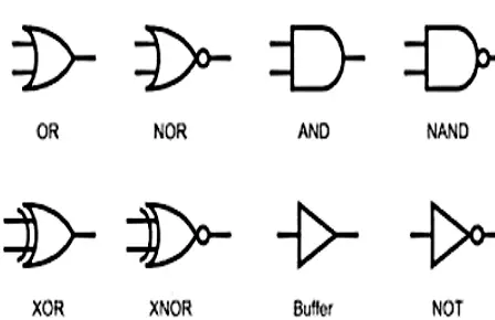
There are 7 basic logic gates:
AND (7408), OR (7432), XOR (7486), NOT (7404), NAND (7400), NOR (7402), and XNOR (74266).
Basic Construction of AND & OR gate from universal gates (NAND and NOR respectively)

We need two NAND gates to create an AND gate. The first NAND gate returns HIGH if either input LOW is or both inputs are LOW. Then the second NAND gate is configured as a NOT gate to invert the output of the first NAND gate.

Similarly, now we need two NOR gates to create an OR gate. The first NOR gate returns LOW if either input is HIGH or both inputs are HIGH. Then the second NOR gate is configured as a NOT gate to invert the output of the first NOR gate.
2.3 LED & 7 Segment Display
A light-emitting diode (LED) is a semiconductor device that emits light when an electric current is passed through it. (Longer Lead – Anode and Shorter Lead – Cathode)
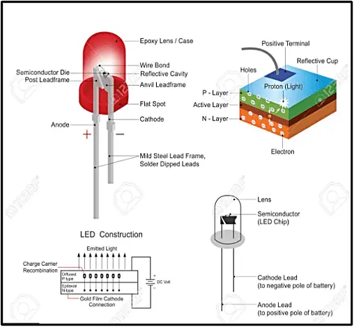
For 7 Segment Display – Refer 2.1.2
3. Experimental Analysis of 4 bit ALU
3.1 Project Pre-requisites
3.1.1 Hardware
Different Logic gates, Mux, Breadboard, 4-bit Binary adder, Decoder driver, 7 segments Led Display wires LED
3.1.2 Software:
Tinker CAD: Having an estimate about the I.C. internal structure and pin diagram of combinational circuits.
Fritzing: Having an estimate about the hardware connections on Breadboard.
Proteus: Having an idea about, how to design the circuit in several stages.
3.2 Some Images of initial tries
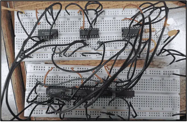
(Fault: NOR gates input get connected in reversed order and Selection of outputs from mux doesn’t take place)
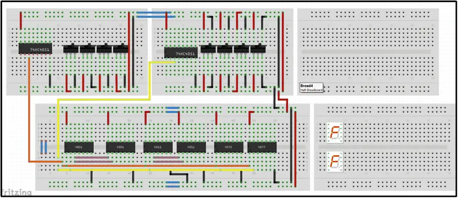
(Fault: Wrong use of concepts while using logic gates, Disadvantage: Some I.C. are not available)
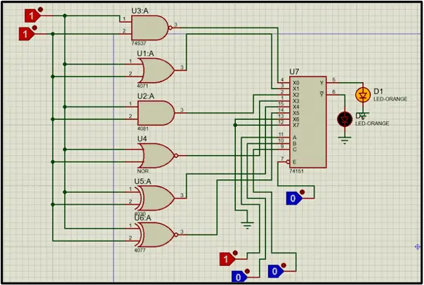
First Successful attempt…
(Advantage: Learn how to design a proper circuit by dividing it in 2-4 subparts, properly understand the working of the whole circuit)
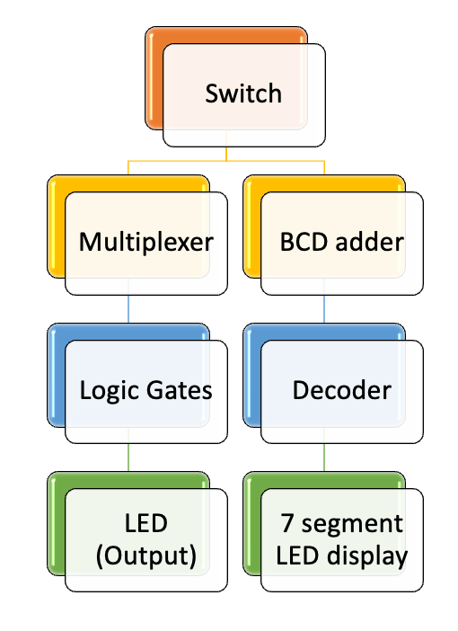
3.3 Block Diagram
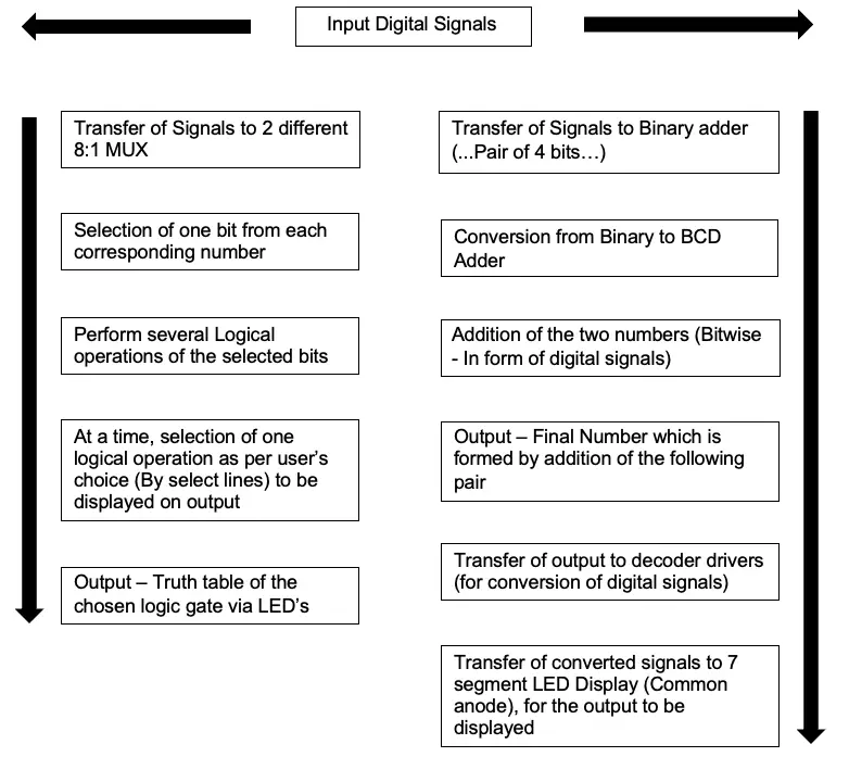
3.4 Flow Chart
3.5 Debugging on Hardware
After having the proper idea about the design and working of the circuit on Proteus software, now the turn comes to put out the circuit on hardware.
This time, a neat and clean circuit was made by us on 3 different breadboards.
Image for the same are provided below:
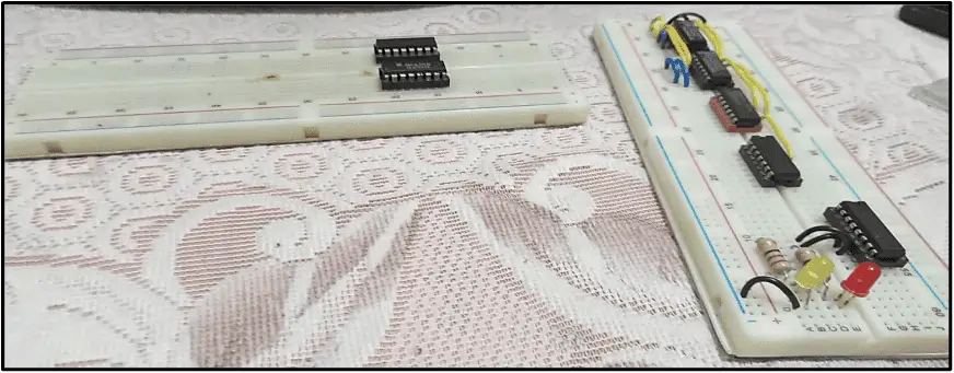
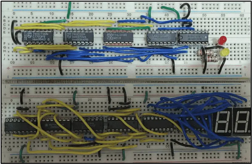

(Fault: Not able to get proper outputs at LED display even after 6 different tries…)
(Final Result: While connecting the 3rd pin of both Decoder drivers to LOW, found that 7 segments LED displays are broken, all 7 led segments are not glowing…)
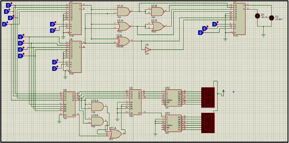
3.6 Final ALU Design
Conclusion
The design of the 4-bit ALU has been designed by using the sub-blocks of decoder driver, 8:1 multiplexer, and gates like NAND, AND, OR, & Inverter, etc…
The ALU performs a total of seven operations, out of which six are logical operations and one is Arithmetical operation. The one arithmetic operation performed is the BCD adder and the six logical operations are AND, OR, XOR, NAND, NOR, XNOR, & NOT.
Future Scope
With the ALU completed, we can now mathematically add and logically process corresponding to any two of the given 4-bit numbers. But this ALU is only a small piece of the puzzle!
For our next steps, we can add a subtractor, could attach a register to the output of the ALU, and feed it back. Then we could create a memory controller that could stream numbers from a chip and perform operations on those numbers. It would be at this point that we could make those numbers stored in memory decide what operation the ALU will do.
This is where it stops becoming an ALU and becomes a simple CPU!!
Credit: The Project on the Analysis of 4 bit ALU is completed by Vasu Singh and Dinesh Joon under the guidance of Dr. Sharda Vashist and Dr. Vandana Khanna, computer science engineering department of NorthCap University, Gurugram, Haryana, INDIA.

Leave a Reply